
The WARP v3 hardware platform has reached end of life and is no longer available. The original product page is archived below.
The Mango team continues to support the 802.11 Reference Design and WARPLab Reference Design for WARP v3 hardware. Technical support is provided via the WARP Forums.
Please contact us with any questions.
WARP v3 Kit
WARP v3 is the latest generation of WARP hardware, integrating a high performance FPGA, two flexible RF interfaces and multiple peripherals to facilitate rapid prototyping of custom wireless designs.
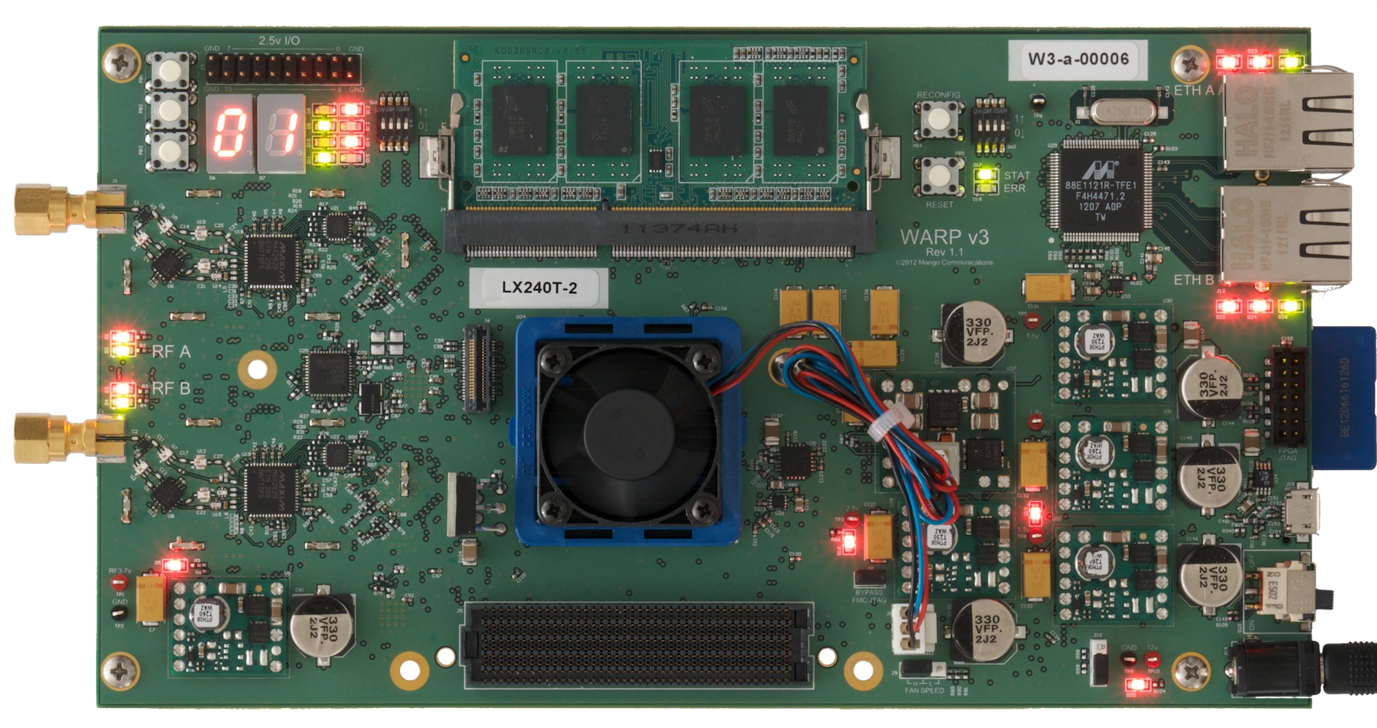
Hardware Features
The hardware features of WARP v3 are listed below. For full details please see the WARP v3 User Guide.
|
|
Reference Designs
We provide a number of open-source reference designs which provide excellent starting points for research projects on WARP v3.
- The Mango 802.11 Reference Design implements the MAC and PHY from 802.11a/g entirely on the WARP v3 node. This design interoperates with commercial Wi-Fi devices in real time. The MAC and PHY source code are provided with the design allowing researchers to customize behaviors at any layer and evaluate their extensions in real networks. The 802.11 Reference Design is available only on Mango WARP v3 hardware.
- The WARPLab Reference Design enables rapid PHY prototyping using WARP hardware for waveform Tx/Rx and MATLAB for signal processing.
- The OFDM Reference Design implements a flexible OFDM PHY and CSMA MAC in the WARP v3 FPGA. This design interoperates with similar designs in previous generations of WARP hardware.
Researchers can also build their custom wireless designs from scratch. We provide a number of open-source support cores which facilitate use of the WARP v3 peripherals and I/O interfaces in custom designs.
Add-on Boards
The WARP v3 hardware can be extended with additional I/O and processing resources via the FMC and Clock Module slots.
- FMC-RF-2X245: Dual-radio FMC module, extends the WARP v3 node to 4-antennas
- FMC-BB-4DA: Quad-DAC FMC module, adds 4 baseband analog outputs
- CM-MMCX: Clock module with MMCX connectors, enables sharing clocks between WARP v3 nodes
- CM-PLL: Clock module with PLL & VCXO, enables simple synchronization of multiple WARP v3 nodes
Many third-party FMC modules are also available.
Kit Contents
The Mango WARP v3 kit contains:
- WARP v3 board (hardware rev 1.1)
- 2GB DDR3 SO-DIMM
- SD card (pre-formatted)
- Power supply (100-240VAC to 12VDC)
- 2 50-ohm SMA terminators
Kit Contents
The WARP v3 kit does not include antennas or RF cables. The RF connectors on WARP v3 are 50-ohm SMA jacks (standard polarity and gender). A wide variety of compatible RF accessories are available from third parties.
The WARP v3 kit also does not include a JTAG programming cable. We recommend the Digilent XUP-USB-JTAG or JTAG-HS2. Both are supported by the Xilinx tools and connect directly to the JTAG connector on the WARP v3 board. It is possible to configure the WARP v3 FPGA using only the SD card. However we strongly recommend having a JTAG cable to enable real-time debugging via the Xilinx SDK and ChipScope Analyzer.